

Graphene (Gr) has been widely investigated in the last years as channel material for high frequency electronics. However, the lack of a band gap in Gr band-structure hinders its application in logic/switching devices and severely limits the performances of high frequency Gr transistors in terms of energy efficiency and power gain.
To overcome these limitations, the research on 2D materials extended to layered semiconductors such as transition metal dichalcogenides (MoS2, MoSe2, WS2, WSe2,..). Furthermore, novel device concepts exploiting vertical current transport in heterostructures of 2D materials with thin insulators or semiconductors have been proposed for ultra-high-frequency (THz) applications. One of the main challenges in this field is the development of scalable approaches for devices fabrication on wafer scale. Among recently demonstrated device architectures, hot electron transistors with a Gr or a MoS2 base, exhibit interesting prospects due to the compatibility of fabrication process with silicon technology.
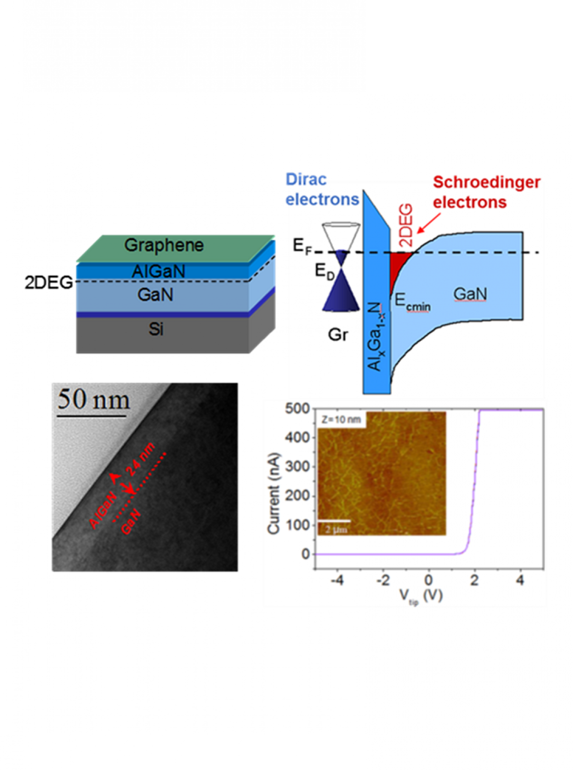
In this context, the integration of 2D materials with wide band gap semiconductors (WBG), such as silicon carbide (SiC) and group III-Nitrides (III-N), i.e. GaN, AlN and related AlGaN/GaN heterostructures, can represent the platform for a new class of transistors with very low power dissipation in the off-state and high operation frequency in the on-state.
The research activity in progress at IMM Catania headquarters is focused on the investigation of several approaches for the integration between 2D materials and WBG semiconductors, with the aim of adding new functionalities to existing SiC and GaN-based devices and of demonstrating novel high frequency transistors. This activity involves several expertise present at IMM, from materials growth (experiment and theory), ab-initio simulation and advanced structural/electrical characterization of interfaces, device fabrication and characterization. Furthermore, it benefits from the interaction with the activities on SiC and GaN processing.

Fig.1 Simulations of Gr growth on SiC: Phys. Rev. E 93, 033304 (2016), and of the electronic transport at the junction between monolayer and bilayer Gr: Phys. Rev. B 86, 235422 (2012).

Fig.2 High resolution electrical characterization by CAFM and structural characterization by STEM of graphene on SiC: ACS Nano 7, 3045–3052 (2013).

Fig.3 Graphene-based field effect transistor: Journal of Crystal Growth 393, 150–155 (2014) .
The main topics under investigation are:
- Growth of epitaxial Gr on hexagonal SiC with different crystallographic orientations and realization of Gr heterostructures with III-N layers (by transfer of Gr grown on catalytic metals to III-N surface or by direct growth of Gr on III-N ).
- Kinetic Monte Carlo simulations of Gr growth on different substrates (SiC. AlN, GaN,..) and ab-initio simulation of transport properties in practical devices.
- Investigation of the interfaces structural/electrical properties by high resolution characterization techniques (SPM, TEM,..).
- Development of processes (2D materials transfer, Ohmic and Schottky contacts, doping, high-k dielectrics deposition by ALD,..),fabrication and characterization of device prototypes based on 2D materials/WBG heterostructures.
These activities are carried out within a network of international collaborations with academic and industrial partners and are currently funded by two EU projects (GraNitE and GRIFONE) within the FlagERA program.