
Owing to its superior electrical properties, such as a wide band gap (3.2 eV) and a high critical electric field (3MV/cm), Silicon Carbide (4H-SiC) is now considered the...
Micro/Nano Electronics
The research activities in the area of Micro/Nano Electronics at IMM Headquarters in Catania cover several aspects, going from materials and processing for power electronics devices (with a focus on wide band gap semiconductors), to advanced experimental and computational methodologies for nanoelectronis, to the implementation of novel materials/processes (e.g., piezoelectric materials, phase-change-materials, alternative doping methods, etc.) for flexible electronics, memories and photonics applications.
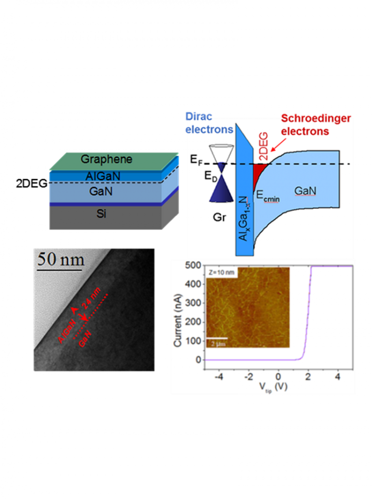
In the field of power and high frequency devices, IMM Headquarters in Catania has a long standing and recognized experience on wide band gap (WBG) semiconductors Silicon Carbide (SiC) and Gallium Nitride (GaN). Fundamental issues and technological aspects related to SiC and GaN power devices are addressed, including the epitaxial growth process of different SiC polytypes, the study of transport properties at interfaces in SiC and GaN devices (metal/semiconductors, dielectric semiconductor,…), the development and characterization of new processes for SiC and GaN devices, etc. The research approach includes the use of several analytical techniques and clean room fabrication of devices and test-patterns, in order to correlate the fundamental material properties with the processing/devices behavior and their reliability. The activity also explores the possibility to integrate 2D-materials (like graphene and related materials) on WBG semiconductors for novel devices operating at high frequency.
The contribution in the field of flexible and large area electronics is devoted to the growth of active compound by low temperature and up-scalable approaches. Piezoelectric stacks based on AlN layers are deposited by low temperature reactive sputtering on PEN, PI, Kapton substrates and implemented in piezocapacitors with strategies addressed to get high d33 values. The activity on flexible devices also extends to 2D-materials, focusing on the fabrication of electronic/optoelectonic devices and sensors on plastic substrates, as well as on the optimization of transfer and deposition methods for CVD-grown-graphene. The theoretical/computational activity employs density functional theory and quantum transport calculations, as well as process simulations, to study the structural, electronic and kinetic properties of the 2D-materials. In the same context, plasma approaches are exploited to grow advanced materials, such as α-Si, SiC, oxynitrides/oxycarbides SiOxNyCz, suitable for low temperature applications on flexible and low cost substrates.
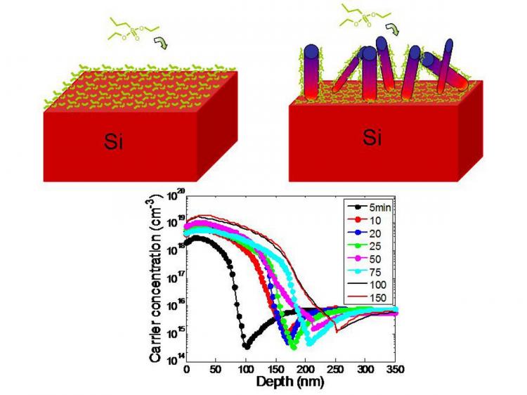
Finally, in the field of devices for classic and quantum information storage and processing IMM Headquarters contributes with the development of new materials, processes and computational methods. Phase changes materials (like GeSbTe alloys) are studied both under the structural and electrical point of view for applications in memories and trimmable resistors, considering also their stability under ion-irradiation. Other aspects under investigation are related to the development of experimental and computational methodologies for nanoelectronics, with a focus on the alternative doping process for semiconductor devices (like monolayer doping process, the plasma immersion ion implantation, and the laser annealing). In this context, computational models are developed to obtain the process control customizing the parameters. Advanced characterizations include also electrical analyses to understand the basic physical mechanisms of the dielectric breakdown (BD) in advanced CMOS circuits.
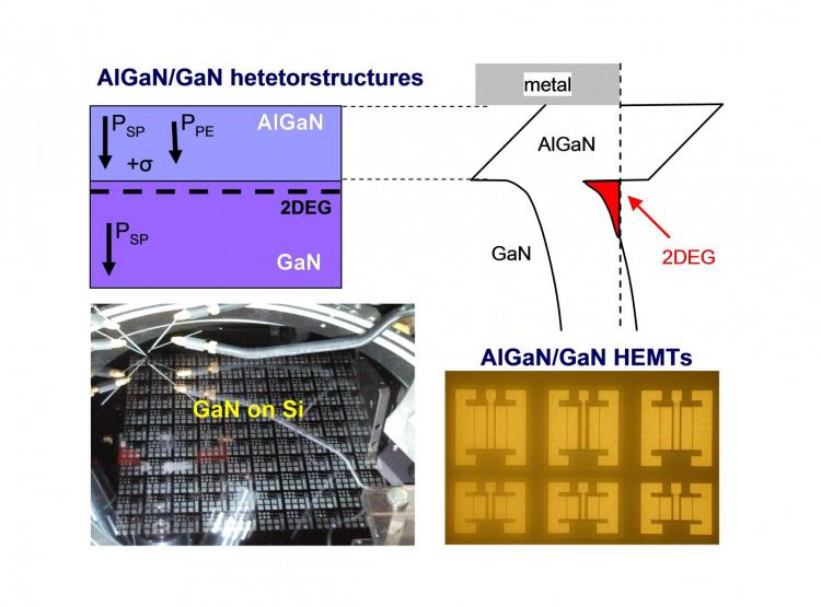
Gallium Nitride (GaN) and its related AlxGa1-xN ternary alloys have excellent properties (like a wide band gap, a high critical electric field and a high electron saturation...
Giuseppe D'Arrigo, CNR-IMM Catania
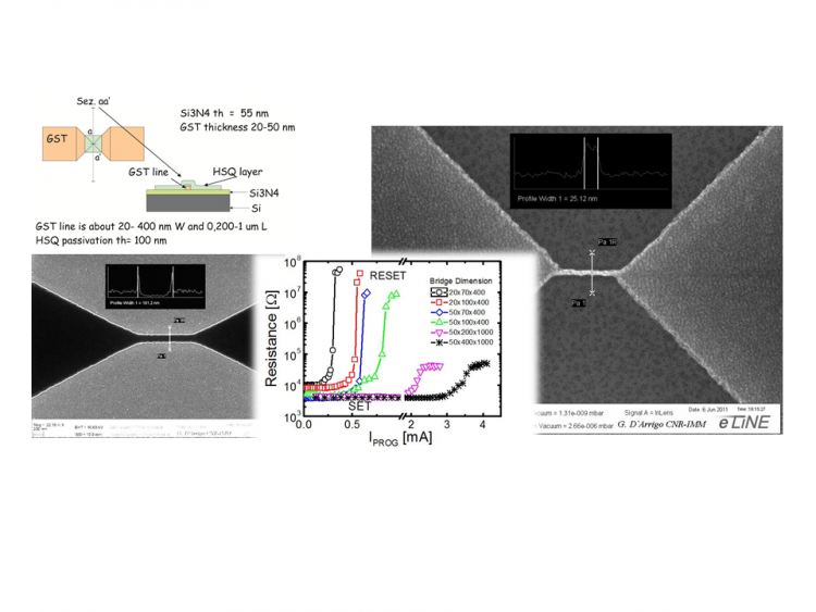
The working principle of a Phase Change Memory (PCM) cell exploits the reversible...
Phase change materials
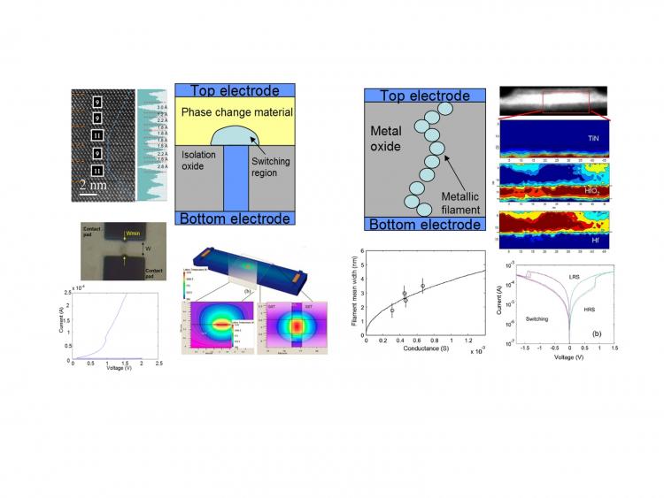
Phase change materials are interesting candidates for emerging applications in memories, photonics, displays, ovonic threshold switch selectors and non von Neumann...
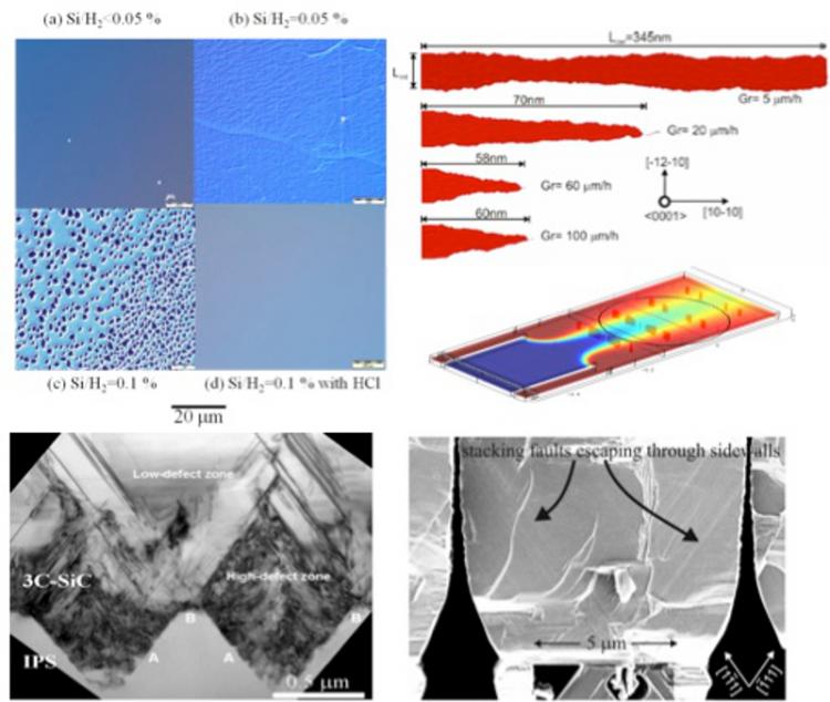
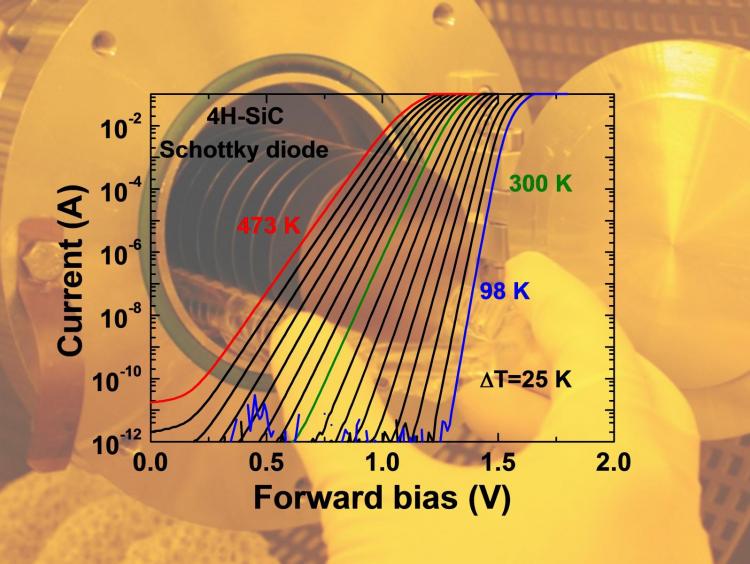
In the actual Power Devices market, 4H-SiC is the emerging material. The main limitations for an extensive application of this SiC polytype in many power applications are the cost of the material...
The demand for low voltage, low power, high performance and increased functionalities has issued severe challenges for the integration progress of nanoelectronic devices so new disruptive...
Graphene (Gr) has been widely investigated in the last years as channel material for high frequency electronics. However, the lack of a band gap in Gr band-structure hinders its application in...

Salvatore Lombardo, CNR-IMM, Catania
The definition of the basic physical mechanisms of the dielectric breakdown (BD) phenomenon is still an open area of research. In...