

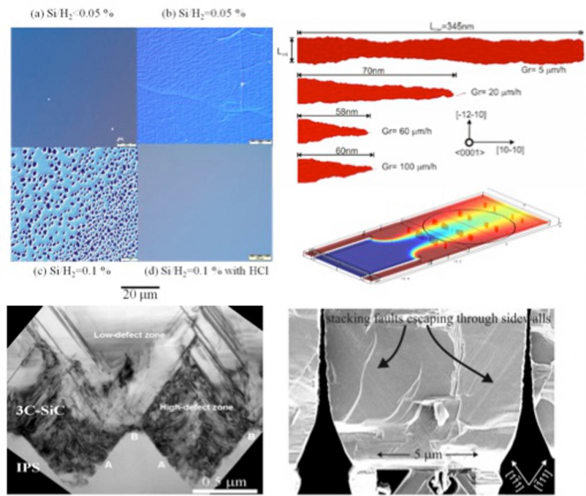
In the actual Power Devices market, 4H-SiC is the emerging material. The main limitations for an extensive application of this SiC polytype in many power applications are the cost of the material and the high defect density with respect to silicon. Then our activity is essentially focused to solve these points by the introduction in the epitaxial process of new chloride precursors that can reduce the cost of the epitaxial process by the increase of the growth rate and then of the throughput of the epitaxial reactors of an order of magnitude (Fig. 1 ).
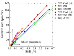
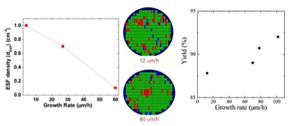
This high growth rate process can also help to reduce the high defect density of the substrates in the active region of the devices, through a no-equilibrium growth. In this way it is possible to obtain at the same time a reduction of one of the major cost of the device process and a large reduction of the defects in the epitaxial layer with a large increase of the devices yield (Fig. 2).
This activity, started in 2003, has produced a large impact on the SiC technology, thanks also to the close connection between experiments, simulations of the growth and new characterization techniques.
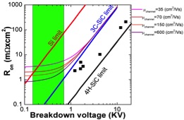
Another important field of research of our group is related to the growth of 3C-SiC on silicon. In fact, the cubic polytype of SiC is extremely interesting because can grow on silicon substrate and in this way a large reduction of the cost of the wafer can be obtained together with the grow on large substrates. Furthermore, the lower band-gap of 3C-SiC (2.2 eV) with respect to 4H-SiC (3.2 eV) can be interesting because this new material can be used in devices with lower breakdown voltages and lower Ron with respect to 4H-SiC and with higher breakdown voltages with respect to silicon. These devices in the range of breakdown voltages between 200 and 900 V will be extremely important in the future because will be used in the electric cars that will be the main application of power devices in the next future (Fig. 3).
The main limitation for this technology is the large difference in the lattice constants between the two materials (20%) and the difference in the thermal expansion coefficient (8%) that produce a large number of defects and a high stress of the material. To solve these problems we are developing new compliance substrates that can help both in the reduction of defects and in the reduction of stress. Furthermore, the use of high growth rate processes can further reduce the defects and produce a high quality material.
These materials cannot be used only for high power applications but also for high temperature MEMS, high temperature photovoltaic cells and detectors for high-energy particles.