

The demand for low voltage, low power, high performance and increased functionalities has issued severe challenges for the integration progress of nanoelectronic devices so new disruptive architectures with 3D schemes have been proposed. In this context conventional doping methods have shown limitations, not yet overcome despite the technological developments, such as use of expensive equipments and materials, need of numerous steps to obtain conformality, formation of structural defects or precipitates and limited control on ultra-shallow diffusion depth. Recently alternative doping processes have been proposed in literature: the molecular monolayer doping (MD), the plasma immersion ion implantation (PIII) and the laser annealing (LA).
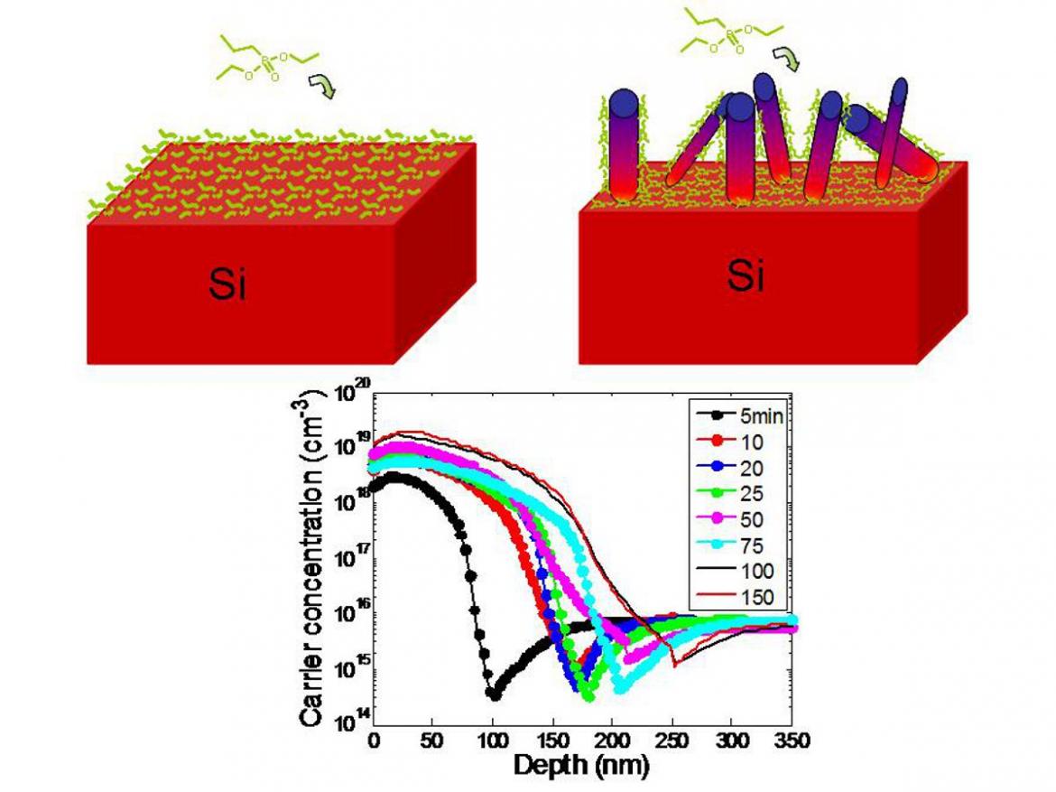
MD shows many advantages: it does not introduce structural defects inside the substrate, it can be used both for of n and p type doping, it provides conformality, it does not use dangerous and expensive sources and it allows to control the junction depth at a nanometer level. The process is based on the self-assembling of a molecular monolayer of specific dopant precursors on the Si substrate. Then an annealing step is used to release the dopant atoms from the layer and diffuse them into the substrate.
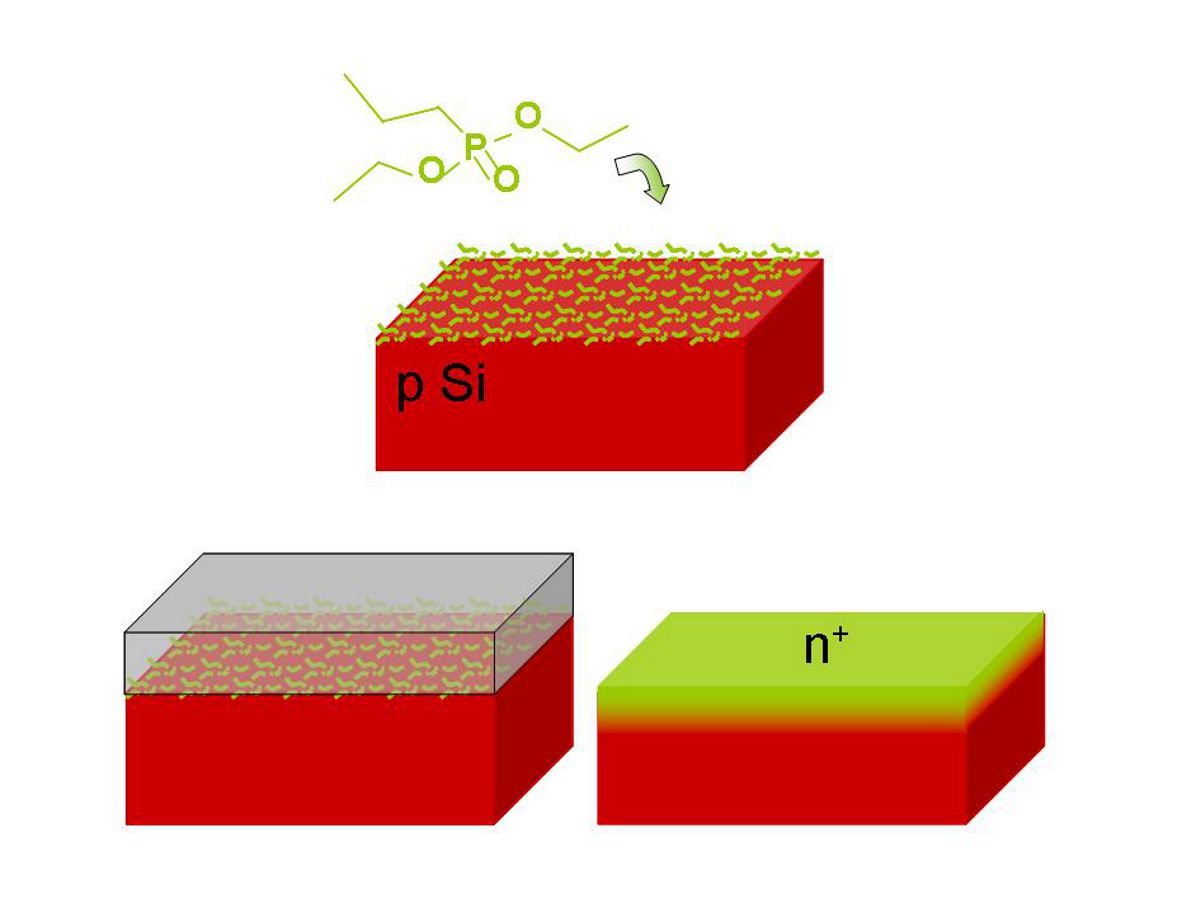
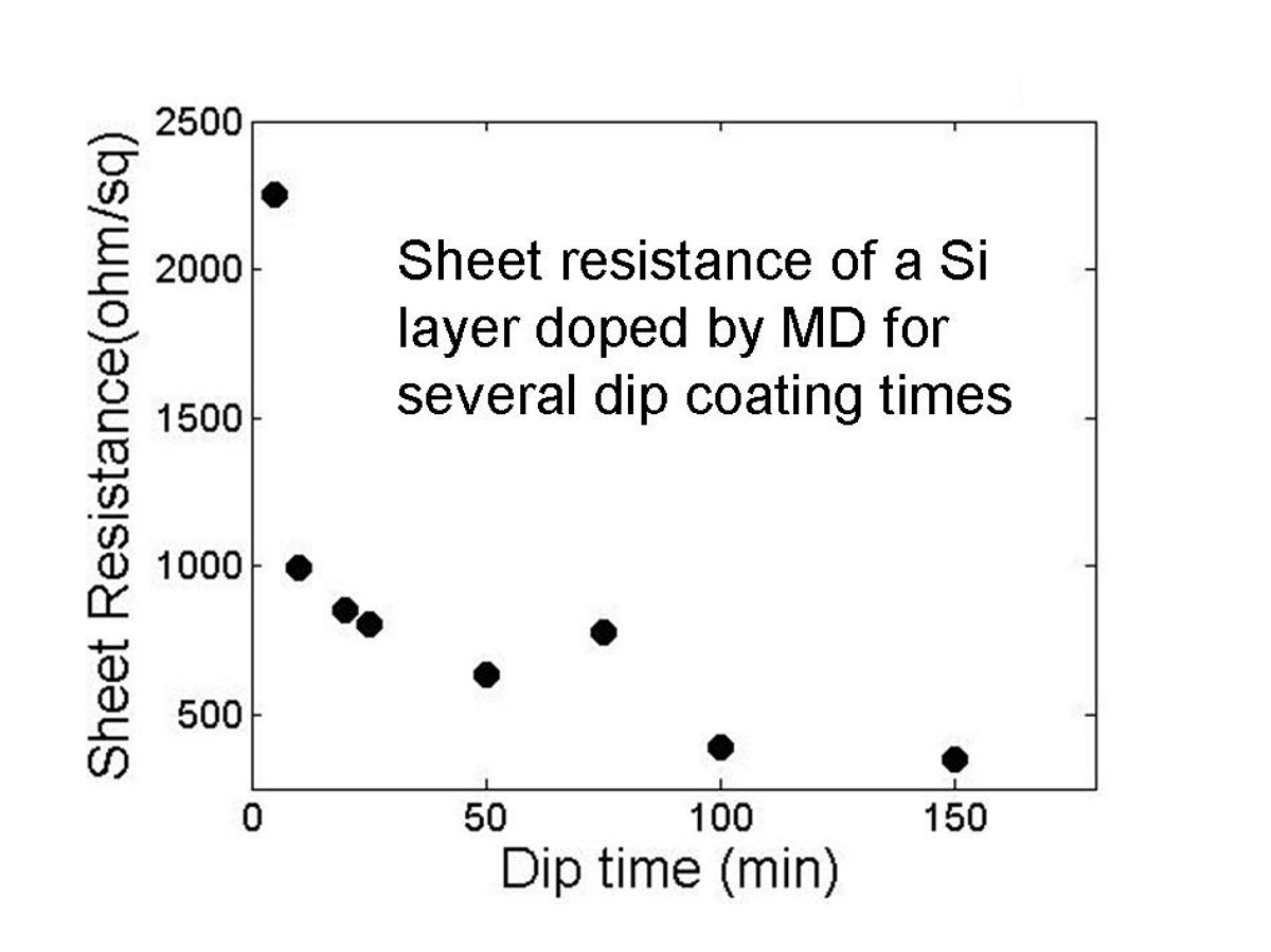
A strong focus of this part of the activity is on the study of the monolayers formation and on the morphological, chemical and electrical characterization of the doped samples, particularly on the sheet resistance values obtained exploring several deposition conditions. Thanks to the intrinsic possibility to obtain conformal doping this method can be specifically exploited as a processing step in the formation of FinFETs where a Si 3D nanostructure (i.e. SiNWs) is integrated in the source/drain region of the device.
Current collaborations on the MD activity (R. Puglisi):
(1) STMicroelectronics - Catania Site
(2) Physics Department of Paderborn University (Germany)
(3) Tyndall Research Center (Ireland)
(4) Chemistry Department of the University of Catania
(5) Physics Department of the University of Messina
The MD study at IMM HQ also involves the activity of 3 PhD students, from the Universities of Catania and Messina, dedicated to this topic.
PIII exploits ions generated in a plasma chamber and accelerated by pulsed electric field and the geometry of the processed device plays a crucial role. Computational models (c) of the interaction between plasma components and the device structure can aid the process control customizing the process parameter to the given structure in study.
LA is an innovative annealing technology with many advantages (abrupt junction, localized heating, defect free region, activation above the solubility limit) compared to the conventionally applied ones. In this case the application of the computational methods is fundamental. In particular using suitable implementation we could predict: the local adsorbed radiation in the exposed surfaces, the time dependent thermal field in the nanoseconds range, the evolving molten region, the dopant redistribution and activation and the defect healing.
Contact people: Rosaria A. Puglisi, Antonino La Magna
Selected pubblications:
- “A comprehensive study on the physicochemical and electrical properties of Si doped with the molecular doping method”, Rosaria A. Puglisi*, Sebastiano Caccamo, Luisa D’Urso, Gabriele Fisichella, Filippo Giannazzo, Markus Italia and Antonino La Magna, Feature Article on Physica Status Solidi A, 212, No. 8, 1685–1694 (2015).
- “Towards Ordered Silicon Nanostructures through Self-Assembling Mechanisms and Processes”, R. A. Puglisi*, Review Article on Journal of Nanomaterials, Volume 2015 (2015), Article ID 586458, 20 pages.
- “Silicon doped by molecular doping technique: Role of the surface layers of doped Si on the electrical characteristics”, Sebastiano Caccamo, Rosaria A. Puglisi*, Salvatore Di Franco, Luisa D’Urso, Valeria Indelicato, Markus Italia, Salvatore Pannitteri, Antonino La Magna, Materials Science in Semiconductor Processing, Volume 42, Part 2, February 2016, Pages 200-203, doi:10.1016/j.mssp.2015.08.017.
- “Electrical characterization of silicon doped by Molecular Doping method”, V. Indelicato, S. Caccamo, E. Fazio, A. La Magna, R. A. Puglisi, Activity Report 2016 ISSN 2038-5889, Dipartimento di Scienze Matematiche ed Informatiche, Scienze Fisiche e Scienze della Terra, pages 97 – 100, (2016).