

Owing to its superior electrical properties, such as a wide band gap (3.2 eV) and a high critical electric field (3MV/cm), Silicon Carbide (4H-SiC) is now considered the material of choice for the next generation of power electronics devices. In particular, 4H-SiC devices can find application in renewable energy conversion systems, hybrid/electric vehicles, high-power industrial and motor drives, power supplies for consumer electronics, etc.
Nowadays, while a variety of 4H-SiC devices (e.g., Schottky diodes and MOSFETs) are already commercially available, there are still several physical/technological issues hindering the full exploitation of the material.
The research activity carried out at IMM Catania headquarters is aimed to address the current limiting issues for SiC devices performances and study new process solutions. A special focus of this research is put on the study, optimization and characterization of interfaces (metal/SiC, dielectric/SiC,…) in practical devices. The main aspects currently object of investigation are:
- Metallizations (Ohmic and Schottky contacts) on different SiC polytypes
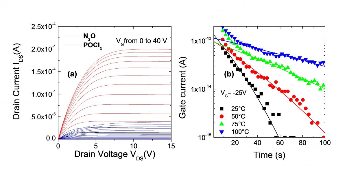
- SiO2/4H-SiC interfaces processing and characterization for high-mobility MOSFETs
- Synthesis and characterization of novel high-k dielectrics for SiC devices
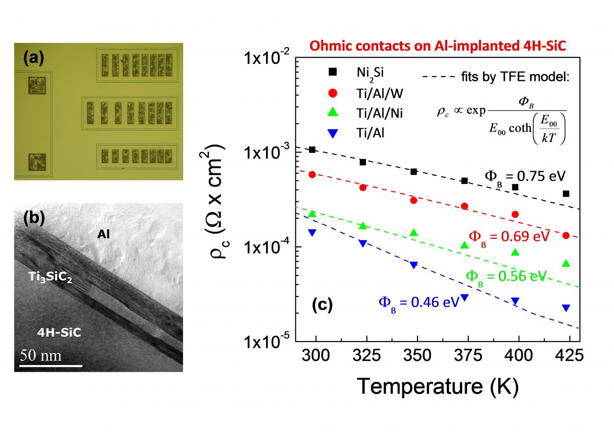
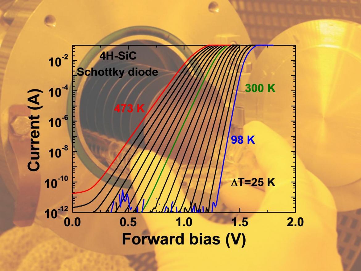
The studies are carried out either on blanket samples and on devices/test-patterns (capacitors, diodes, transistors, TLM, VdP structures, etc.), using a large variety of characterization techniques. The conventional characterizations are often combined with nano-scale electrical measurements, employing scanning probe microscopy (SPM) to assess fundamental interface properties, such as homogeneity of Schottky barriers, uniformity of dopant profiles, activation phenomena in nitrated interfaces, local breakdown events in gate oxides, etc.
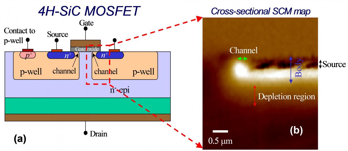
In the last years, this activity produced important contributions to the understanding of the mechanisms limiting the channel mobility in 4H-SiC MOSFETs subjected to different post-oxidation-annealing processes, and to the explanation of the “counter doping effect” in the MOSFET channel during these thermal treatments. Reliability aspects related to the threshold voltage instability and high-k dielectrics for 4H-SiC MOSFETs are also under current investigation.
The group has an internationally recognized experience in SiC device processing technology and characterization. In the last decade, the activity has been carried out collaborating with several academic and industrial partners in the framework of different National and European projects: MANSiC (2007-2010), Ambition Power (2010-2014), Last Power (2010-2014), NetFISiC (2011-2015), Challenge (2017-2020), WInSiC4AP (2017-2020).
Reference person: Fabrizio Roccaforte
Involved personnel: Patrick Fiorenza, Giuseppe Greco, Filippo Giannazzo, Raffaella Lo Nigro, Salvatore, Di Franco, Domenico Corso, Emanuela Schilirò, Monia Spera, Fabrizio Roccaforte