

Salvatore Lombardo, CNR-IMM, Catania
The definition of the basic physical mechanisms of the dielectric breakdown (BD) phenomenon is still an open area of research. In particular, in advanced CMOS circuits, the BD of gate dielectrics occurs in the regime of relatively low voltage and very high electric field; this is of enormous technological importance, and thus widely investigated but still not well understood. Such BD is characterized by a gradual, progressive growth of the gate leakage through a localized BD spot. We work both on the experimental and on the modeling side to provide understanding of the main physical mechanism responsible for the progressive BD growth. We demonstrate the ability to control the breakdown growth rate of a number of gate dielectrics and provide a physical model of the observed behavior, allowing to considerably improve the reliability margins of CMOS circuits by choosing a correct combination of voltage, thickness, and thermal conductivity of the gate dielectric.
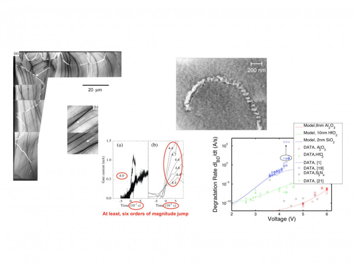
In the figure we show TEM images demonstrating that for thick oxides during BD, BD point propagates laterally along lines along the MOS surface. The lines are actually done by individual BD spots, suggesting the presence of numerous precursor defects of percolation paths. As oxide thickness (and stress voltage) decrease, the lateral migration of the BD spot does not occur anymore, and as the voltage is scaled low enough there is a sudden transition to a slow BD spot growth, the progressive BD regime. Progressive BD appears a general phenomenon, experimentally observed in various gate stacks: poly-Si / SiON / Si; MG / hi-k / Si; MG / hi-k / InGaAs;
The purpose of the activity is to study the physical mechanisms of dielectric breakdown in dielectrics for high performance / low power CMOS. The activity is at the moment focused to the case of gate dielectrics in planar CMOS, also including the case of oxides on III-V substrates. The plan is to extend the study to the case of MEOL and FEOL.
Selected Papers
Lombardo, S; Stathis, JH; Linder, BP; Pey, KL; Palumbo, F; Tung, CH, Dielectric breakdown mechanisms in gate oxides, JOURNAL OF APPLIED PHYSICS, 142, 2005, 98, 12, 121301, 10.1063/1.2147714
Linder, BP; Lombardo, S; Stathis, JH; Vayshenker, A; Frank, DJ, Voltage dependence of hard breakdown growth and the reliability implication in thin dielectrics, IEEE ELECTRON DEVICE LETTERS, 74, 2002, 23, 11, 661, 663, 10.1109/LED.2002.8050
Lombardo, S; La Magna, A; Spinella, C; Gerardi, C; Crupi, F, Degradation and hard breakdown transient of thin gate oxides in metal-SiO2-Si capacitors: Dependence on oxide thickness, JOURNAL OF APPLIED PHYSICS, 67, 1999, 86, 11, 6382, 6391, 10.1063/1.371701
Lombardo, S; Stathis, JH; Linder, BP, Breakdown transients in ultrathin gate oxides: Transition in the degradation rate, PHYSICAL REVIEW LETTERS, 28, 2003, 90, 16, 167601, 10.1103/PhysRevLett.90.167601
Pagano, R; Lombardo, S; Palumbo, F; Kirsch, P; Krishnan, SA; Young, C; Choi, R; Bersuker, G; Stathis, JH, A novel approach to characterization of progressive breakdown in high-k/metal gate stacks, MICROELECTRONICS RELIABILITY, 19, 2008, 48, 11-Dec, 1759, 1764, 10.1016/j.microrel.2008.07.071
Stathis, JH; Linder, BP; Rodriguez, R; Lombardo, S, Reliability of ultra-thin oxides in CMOS circuits, MICROELECTRONICS RELIABILITY, 18, 2003, 43, 09-Nov, 1353, 1360, 10.1016/S0026-2714(03)00242-7
Lombardo, S, Intrinsic dielectric breakdown of ultra-thin gate oxides, MICROELECTRONIC ENGINEERING, 15, 2001, 59, 01-Apr, 33, 42, 10.1016/S0167-9317(01)00632-3
Privitera, S; Bersuker, G; Lombardo, S; Bongiorno, C; Gilmer, DC, Conductive filament structure in HfO2 resistive switching memory devices, SOLID-STATE ELECTRONICS, 0, 2015, 111, 161, 165, 10.1016/j.sse.2015.05.044
Palumbo, F; Lombardo, S; Eizenberg, M, Physical mechanism of progressive breakdown in gate oxides, JOURNAL OF APPLIED PHYSICS, 3, 2014, 115, 22, 224101, 10.1063/1.4882116
Privitera, S; Bersuker, G; Butcher, B; Kalantarian, A; Lombardo, S; Bongiorno, C; Geer, R; Gilmer, DC; Kirsch, PD, Microscopy study of the conductive filament in HfO2 resistive switching memory devices, MICROELECTRONIC ENGINEERING, 14, 2013, 109, 75, 78, 10.1016/j.mee.2013.03.145