

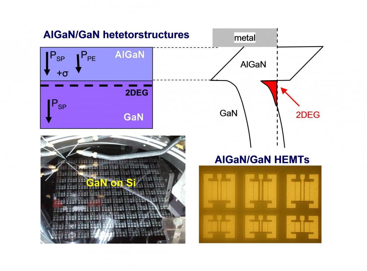
Gallium Nitride (GaN) and its related AlxGa1-xN ternary alloys have excellent properties (like a wide band gap, a high critical electric field and a high electron saturation velocity) making them suitable semiconductors for high power and high frequency devices. In particular, due to the presence of the two dimensional electron gas (2DEG) generated by the spontaneous and piezoelectric polarization charges, AlGaN/GaN heterostructures can be used for the fabrication of high electron mobility transistors (HEMTs).
The research activity carried out at IMM Catania headquarters is focused on fundamental aspects related to lateral and vertical GaN-based devices, i.e., spanning from the development and characterization of the elementary device building blocks (contacts, gate dielectrics, etc.), to their integration and impact into the device behavior, considering also the role of the material quality. The involved team holds a multidisciplinary background (physics, chemistry, electronic engineering and material science) and expertise on GaN materials and devices.
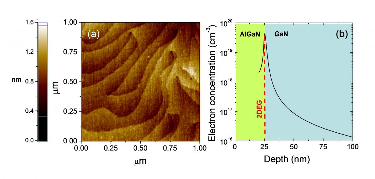
The work is performed on a variety of substrates including large-area Si, SiC, and sapphire, with a view towards “free-standing” GaN for novel vertical devices concepts. The incoming GaN-based epilayers and AlGaN/GaN heterostructures are characterized in terms surface morphology, electrically active dislocations density, sheet carrier density and mobility of the 2DEG, etc. The activity includes not only the physical characterization of materials and processes, but also the fabrication of devices and test patterns (i.e., Schottky, MIS capacitors, TLM and VdP, HEMTs, MISHEMTs, ...) for advanced electrical analyses.
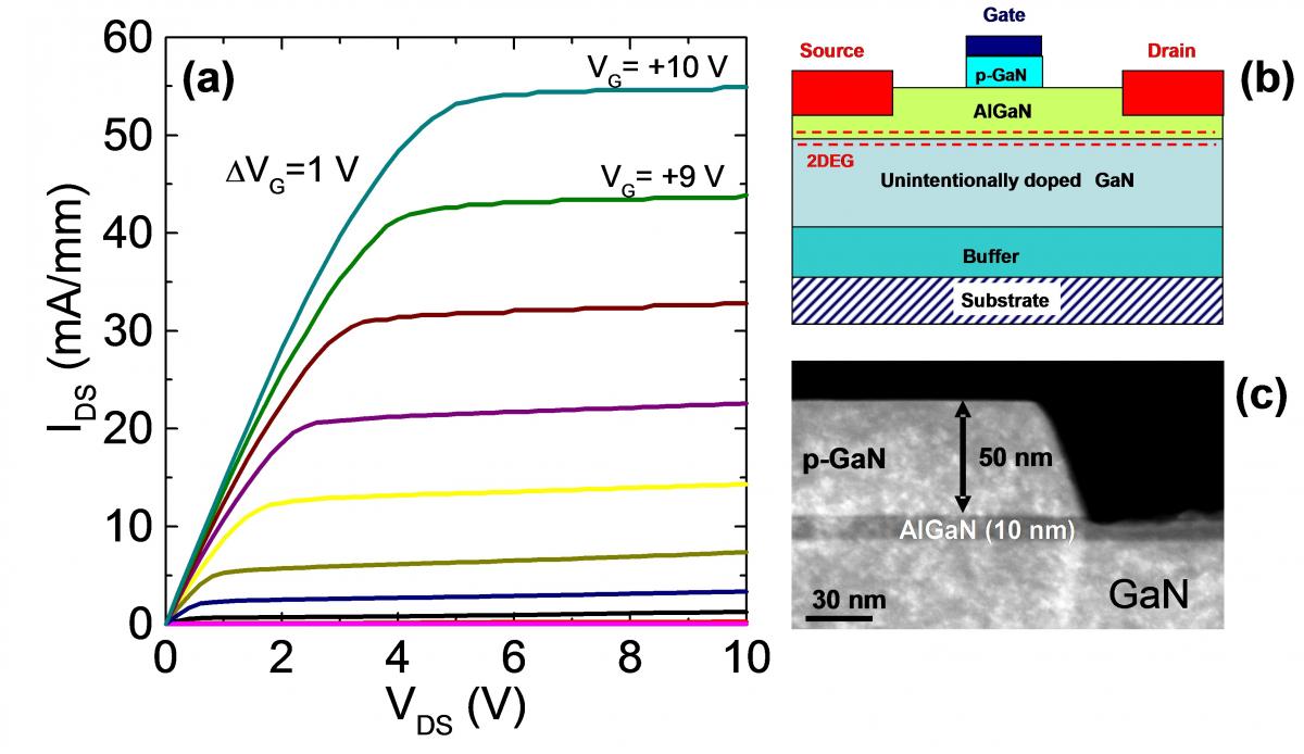
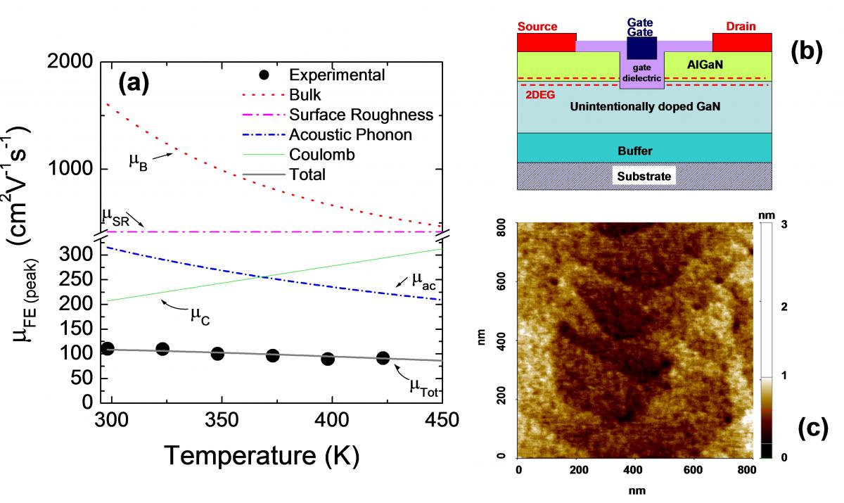
In the last years, extensive studies on contact technology and normally-off HEMTs with a p-GaN gate have been carried out. Moreover, the conduction mechanisms and trapping phenomena in recessed hybrid MISHEMTs have been investigated. Activity on the synthesis, characterization and integration of dielectrics and nano-laminates by ALD is also carried out to limit gate leakage and current collapse effects in GaN devices.
The group has several national and international collaborations with industrial and academic institutions, developed in the last years through the participation in National and European research programs: Ambition Power (2010-2014), Last Power (2010-2014), GraNitE (2016-2019), ETNA - Cooperation Agreement CNR-PAS (2017-2019).
Reference person: Fabrizio Roccaforte
Involved personnel: Giuseppe Greco, Patrick Fiorenza, Filippo Giannazzo, Raffaella Lo Nigro, Salvatore Di Franco, Domenico Corso, Emanuela Schilirò, Monia Spera, Fabrizio Roccaforte