

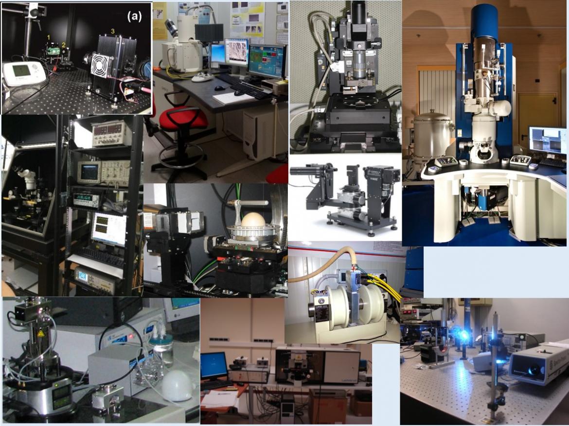
The characterization of a material is the measurement of at least one of its structural, morphological, electronic and physical properties. Device characterization include the understanding of its processing, working principle, and performances. CNR-IMM Headquarters staff members have a strong background in the characterization of materials and devices of interest in the microelectronic field. They have strong relations with industries and often provide technical advices (under NDA) for materials and devices processing.
The researchers experience is focused on materials and devices of interest in microelectronics. Non-limiting examples are Si, SiC, Graphene, GaAs, different nanomaterials like nanodots, Si nanowires, C nanotubes, etc.. Microelectronic, optoelectronics and devices for energy conversion, obtained from their processing are also widely characterized. The techniques available in the laboratories allow the researchers to obtain electrical, optical and structural information. The first can be obtained from single molecules to devices on 8 inches wafers, in a wide temperature, voltage, current and frequency range. Morphological/structural techniques allow obtaining information at atomic level (nanometer resolution or below) on the material structural and morphological properties. Optical techniques are non-destructive, fast, requiring very little sample preparation and can be performed at room temperature and atmosphere.
Carbon based nanomaterials Lab - Ref.: S. Scalese (silvia.scalese@imm.cnr.it)
The Laboratory is dedicated to carbon based nanostructures and includes synthesis and processing facilities along with different characterization tools.
The characterization techniques available in the laboratory are listed below:
- Scanning electron microscope
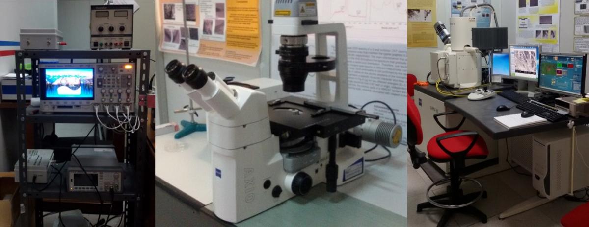
Lab is equipped with a ZEISS SUPRA 35 scanning electron microscope (SEM) with a Schottky field emission gun. The acceleration voltage can be varied in the 0.1 – 30 kV range. The instrument achieves a spatial resolution of 1 nm at 20 kV and is equipped with three different detectors: in-lens detector for secondary electrons, E-T chamber detector, and a detector for backscattered electrons.
A nano-manipulator system is also installed inside the chamber for electrical measurements on nanometer structures during SEM observations. It includes a Keithely sub-femtoamp remote source-meter instrument 6430.
An energy dispersive X-ray (EDX) analysis system (Oxford AZtecENERGY Advanced) with a X-MAX 80 mm2 detector is inside the SEM chamber, allowing to perform chemical mapping of the samples.
- Optical microscope
An inverted microscope Zeiss Axio Vert A1 working in both reflection and transmission, with LED illumination, and 10x, 20x, 50x objectives, allows bright field and fluorescence analysis.
- Electrical characterization tools
Digital Oscilloscope with 4 channels, 100MHz, Agilent DSO-X-2014°
Function Generator 2 channels, 30MHz, Agilent 33500B
Function Generator 4 channels, PC-controlled, programmable, 1MHz 20Vpp/channel, Elbatech
Power supply 2 channels, 30V 3A/channel, ISO-TECH IPS 2303
Digital Multimeter ISO-TECH IDM 66RT
Sub-Femtoamp Remote Sourcemeter SMU Keithley 6430
- High precision balance (A&D HR202i semi microbalance) with ultra fine 0.01 mg resolution in the 0-42g range.
- Spectroradiometer (Avaspec 2048L AVANTES): measurements of spectral irradiance (wavelength range: 178-1150 nm), reflectance and transmittance
Electrical Measurements Lab – Ref.: S. Lombardo (Salvatore.lombardo@imm.cnr.it)
Lab is equipped with three probe stations for measurements on 6, 8, and 12 inches wafers. One probe station is equipped with three-axial Kelvin contacting system and Attoguard shielding system by Cascade Microtech for current and voltage measurements with very low noise. It is also possible to carry out electrical measurements as a function of temperature from 65 to 200 °C on the 8 inches probe station, current measurements in the 1 fA – 10 A range, and voltage measurements in the 10 µV – 1100 V range. The instruments allows us to carry out electrical measurements with a time resolution as low as few nanoseconds, and the laboratory is equipped with a network analyzer for frequency measurements up to 20 GHz.
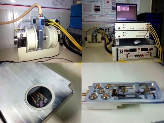
Hall Measurements equipment – Refs.: D. Corso, F. Roccaforte (domenico.corso@imm.cnr.it; fabrizio.roccaforte@imm.cnr.it)
The variable temperature MMR Hall Effect Measurement System provides automatic measurements of the electrical properties of semiconductor materials (resistivity, carrier density. mobility) using the Van der Pauw measurement technique. The sample is mounted in a vacuum chamber on a computer controlled thermal stage. The MMR Programmable Temperature Controller allows an operating temperature range from 300 K to 730 K. A Hall Measurement Controller, coupled with an electromagnet, controls both the magnetic field strength (up to 5000 Gauss) and direction. A spring loaded probe assemblies provide the electrical access to the sample under investigation without the use of wire bonding or soldered connections. In addition, this system enables a faster sample exchange. The maximum sample mounting surface size is 10mm x 12mm.
High angular resolution X-ray equipment – Ref.: A. Alberti (alessandra.alberti@imm.cnr.it)
D8discover made by Bruker-AXS. The main body consists of a horizontal high resolution goniometer (0.0001°) and of a ¼ Eulerian Cradle which enable to perform out of plane and in plane investigations of the lattice structure. The source is a 3 kW Cu long fine focus tube equipped with a 40 nm Goebel mirror. Medium and high resolution are assured by an Asymmetric 4-Bounce Ge(220) and a Symmetric 4-Bounce Ge(440) monocromators, respectively. The facility is equipped with: a NaI(Tl) scintillator counter and a linear detector (10° of angular aperture); an heating stage for annealing up to 900°; a motorized stage for mapping up to 5.9 inches wafer diameter. Out of plane configuration allows to perform: X-ray diffraction (XRD); high resolution X-ray diffraction (HR-XRD); grazing incidence diffraction; X-ray reflectivity (XRR); reciprocal space mapping (texture, stress, composition). In plane configuration allows to perform: in plane grazing incidence diffraction (in plane GID); grazing incidence small angle x-ray scattering (GISAXS); reciprocal space mapping.
Micro-nanomachining and Electrochemical lab – Refs.: G. D’Arrigo, A. Sciuto (giuseppe.darrigo@imm.cnr.it; antonella.sciuto@imm.cnr.it)
The micro-nanomachining lab is equipped with the following tools for the characterization of micro and nano scaled materials, devices and physical sensors:
- E-Line Ultra High Resolution Electron-Beam-Lithography and Nano-Engineering Workstation:
In the system are included two Cartesian Nano-manipulators to do local EBIC (Electron Beam Induce Current) characterization under electron-beam or SEM observation.
In the system is included an Piezo-system to monitor resonance frequency of micro-nano structure up to 300Khz under SEM observation.
- Nano-Indenter and Nano-Scratch system CSM to characterize the Young Modulus and Adhesion in nano-scale range.
- PAR apparatus, Potentiostat and Galvanostat system, for electrochemical characterization.
- Quartz Micro-Balance to appreciate monolayer depositions in solution with static condition and under flux cells.
- MITUTOYO Measuring Microscope with in situ reflectivity measurements system, Probe-Station for measurements and four electrical probes for electrical measurements; The stage is also equipped with a PID-controlled heater for in situ annealing of the sample from RT up to 300°C; Piezo-Systems suitable for resonance frequency measurements of MEMS structures.
- Four point sheet resistance apparatus.
- Optical system for electro-optical characterization of photosensor equipped with UV deuterium lamp, band pass filters (in the range from 256 to 405 nm), optical fibers with core diameters 200, 400 and 600 um and focusing system for the irradiation of samples in package or in dye on Probe-Station.
- Probe-Station equipped with a dual channel 2636B keithley SMU, an oscilloscope Tektronix DPO 7104 C and a Pulse Function Arbitrary Generator keysight 81160A.
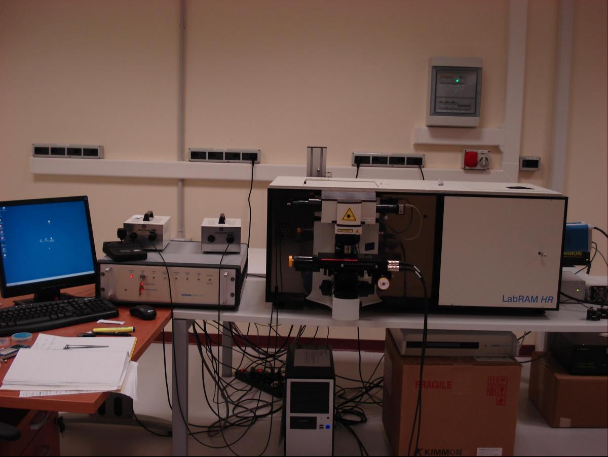
Micro-Raman and Micro-Photoluminescence Lab – Ref.: F. La Via, (francesco.lavia@imm.cnr.it)
The laboratory of Micro-Raman and Micro-Photoluminescence is working essentially on the characterization of 3C-SiC and 4H-SiC. The Horiba Jobin Yvone LabRam 800 system is equipped with a HeCd laser (325 nm) and a HeNe laser (632 nm)
In this lab it is possible to obtain large maps on 4 inches wafers of defects (Stacking Faults, point defects) with a high lateral resolution of about 1 micron.
New techniques for the characterization of stacking faults in 3C-SiC or the effect of defects on the electrical characteristics of devices (Photon Induced Current) has been developed in the last years.
Optoelectronic Lab – Ref.: S. Libertino (sebania.libertino@imm.cnr.it)
The laboratory equipment (listed below) allow performing photoluminescence (PL), electroluminescence (EL), lifetime and near-infrared spectroscopy (NIRS) measurements. Fluorescence measurements on solids or liquids are also performed.
Otpical characterization of devices in fiber is also available.
- Optical tables
- Free space Lasers: Ar multi-lines (4 W); Solid state (405 nm,633 nm); He-Ne (35 mW); picosecond lasers at 405 nm and 633nm
- Fiber optic lasers: solid state (1.55 um); He-Ne (35 mW); picosecond lasers at 405 nm and 633nm
- Incoherent visible and UV light sources
- Mechanical and acusto-optical choppers
- Monochromators (1/2 λ and ¼ λ) equipped with UV-Vis-NIR gratings
- Lock-in system (SR830)
- Liquid N cooled Ge detector (NIR)
- Photomultiplier
- Source-meter-Units (Keithley 236)
- Electrical Pulse generators
- 1 GHz oscilloscope (Tektronics)
- He cooled cryostat computer controlled for low temperature Pl and EL.
- Optical components: piezoelectric and manually controlled translation stage systems; lens and filters in the visible and IR range; single and multimodal optical fibers in the Vis-NIR ranges.
- Small optical benches and components are also available to realize “portable” optical tables.
Photovoltaic Lab – Ref.: S. Lombardo (Salvatore.lombardo@imm.cnr.it)
Bentham per riflettività, QE, trasmittanza nel range 300 2200 nm,
5 laser al ps da 400 a 1 um circa,
probe station cascade da 6’ per misure su fetta da temperatura ambiente a 300°C
sistema di photon counting,
piccola strumentazione: due tavoli ottici, goniometro e due stage motorizzati, etc.
Scanning probe microscopy laboratory -Refs.: P. Fiorenza, F. Giannazzo (patrick.fiorenza@imm.cnr.it, filippo.giannazzo@imm.cnr.it)
The lab is equipped with three atomic force microscopes with complementary properties:
- Dimension D3100 by Digital (now Bruker) with a Nanoscope V controller. It allows tapping mode and contact mode morphological measurements in open and close-loop mode under ambient conditions and on large samples (200 mm wafers). Furthermore, it is equipped with electrical modules for scanning capacitance microscopy (SCM), conductive atomic force microscopy (CAFM), torsion resonant CAFM and scanning spreading resistance microscopy (SSRM). SCM and SSRM measurements have been applied for nanoscale resolution and quantitative profiling of carrier concentration and resistivity in semiconductor materials (Si, SiGe, SiC, GaN, AlGaN) and devices. CAFM (in contact and torsion resonant mode) has been employed for local current mapping at metal/semiconductor and dielectric semiconductor interfaces, as well as for nanoscale electrical characterization of graphene and other 2D materials (MoS2,..), of graphene/semiconductor heterostructures, of polymers and organic materials. Local electrostatic measurements (EFM, KPFM) and magnetic measurements (MFM) can be implemented in this system. The close loop-mode allows also to implement nanolithography.
- Multimode by Digital (now Bruker) with Nanoscope IIIA controller. It allows us to carry out atomic force microscopy measurements with low noise and a very high spatial resolution (atomic level) on small samples (1 cm2). Furthermore, the sample holder is connected to a heating/cooling system, allowing to perform both topography and current (CAFM) measurements from room temperature to 250 °C.
- XE 150 by PSIA (now Park-Instruments). It allows us to get morphological analysis with an interferometer control of the lateral position on the sample surface, either in contact or in true non contact mode. This latter operation mode is especially suitable for non invasive topographic measurements on soft matter samples (such as polymers and organics), as well as for long time characterization of hard surfaces, such as SiC, GaN and AlN, preserving the AFM tip quality. The system is also equipped with the module for CAFM measurements.
Sensor Lab – Ref.: S. Libertino (sebania.libertino@imm.cnr.it)
The laboratory is equipped with the facilities to store and manipulate biological molecules with NO biohazard and to characterize biosensors.
Biological molecules manipulation facilities include:
- Biological fan (NO biohazard) for biological sample preparation
- Refrigerated centrifuge (max speed 6000 rpm)
- Milli-Q ultrapure water system
- Mettler Toledo AG285 high precision balance
- 4°C and -20°C sample storage
- Cary 50 Spectrophotometer (200-1100 nm)
- Small laboratory equipment: pH meters; warmed magnetic stirrer (with temperature control system); vortex mixer; micro-pump for liquids; micropipettes; etc.
Biosensors testing equipment are:
- Probe station with three-axial Kelvin contacting system by Cascade Microtech for current and voltage measurements with very low noise on devices on wafers up to 6 inches.
- Small thermostatic chucks for electrical measurements as a function of temperature from 10 to 500 K on,
- Current measurements can be carried out in the 1 fA – 3 A range, and voltage measurements in the 10 µV – 1100 V range. Time resolution can be as low as few nanoseconds.
- 1 GHz Oscilloscope
- Kulike and Soffa Wire bonder
Optical characterization is performed in the Optoelectronic laboratory.
Small area solar cells characterization – Ref.: R. Puglisi (rosaria.puglisi@imm.cnr.it)
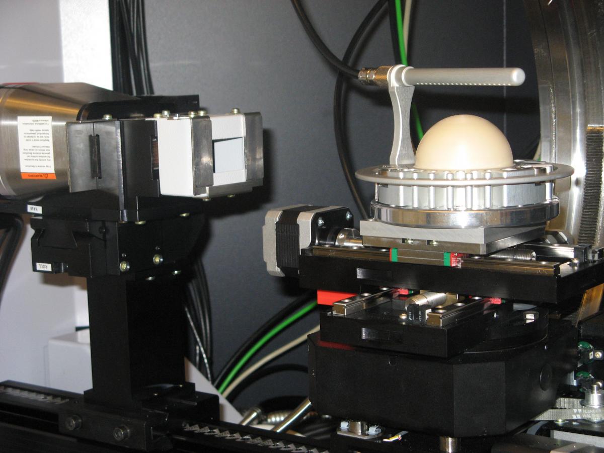
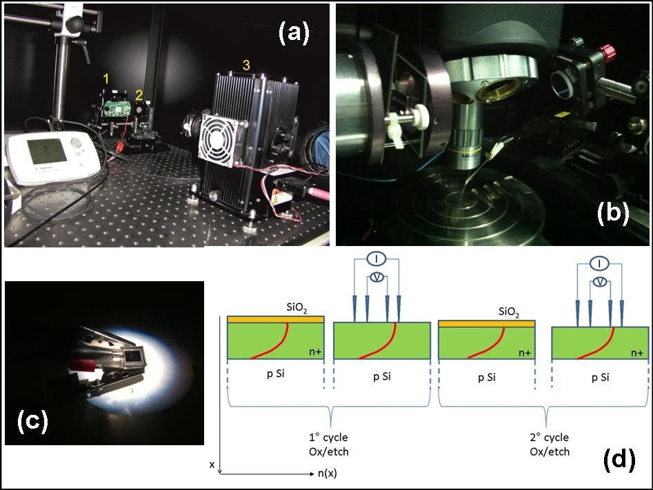
The lab is equipped with two probe stations for measurements on 2 and 6 inch wafers, both equipped with 4 micromanipulators; 1 Solar Simulator (Figure a), with a Xenon lamp, filter AM1.5G, spectral match class A, irradiance up to 200 mW/cm2, beam size 35 mm, beam uniformity class B, temporal stability class A; 1 Monochromator Cornerstone 130 1/8 m, Wavelength Accuracy 0.50 nm, Focal Length 130 mm, 2 Gratings; 2 diode lasers (659 nm, 408 nm) CW and Pulsed Up to 150 MHz – IIIB Class – beam 1 mm – 60/50 mW; 1 Arbitrary Waveform Generator, 15 MHz; 1 electrometer Keithley 6512; 3 SMU Keithley K236; 1 SMU Keithley K237; 1 LCR Meter 4284A; an optical table.
It is possible to carry out current versus voltage (I-V) measurements of solar cells, both on wafers and on packaged devices (Figure b and c), with maximum area 2cm2, in dark and under solar light simulated conditions, in air or under vacuum (50 mTorr), at room temperature and up to 300°C. The I-V characteristics can also be measured as a function of light level and wavelength and up to 100 Suns, on 2mm spot. It has also been recently developed a new methodology based on four-point measurements on doped semiconductor layers progressively removed by controlled chemical etch, the Chemical-4PointProbe (C-4PP), Figure d. The technique allows the sheet resistance profiling with depth resolution of 1.5nm. Dimensions: from 1cm² up to 6-inch wafers. Range of sheet resistances: 10-1 - 103ohm / sq. Measuring environment: vacuum (100mTorr) and in the air.
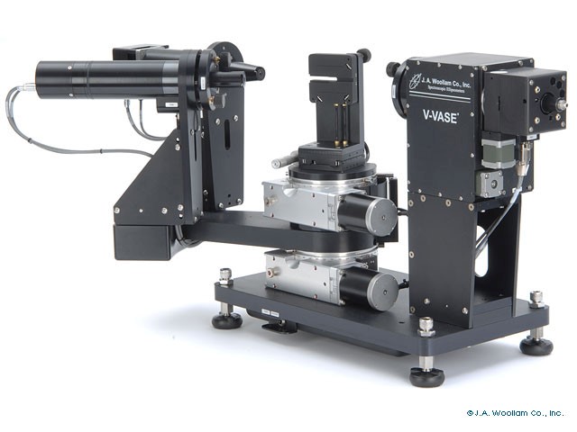
Spectroscopic Ellipsometry Lab – Ref.: G. Mannino (giovanni.mannino@imm.cnr.it)
This Lab is equipped with a J.A.Woollam WASE spectroscopic ellipsometer for measurements of optical constants having specific capabilities and advantages:
- Monochromator for superior wavelength selection. The monochromator is positioned before the sample so only low intensity monochromatic light strikes the sample. This ensures photo-sensitive materials are not altered.
- Vertical sample stage with fixed input unit and independent control of sample and detector angles allows measurement of: Variable Angle Spectroscopic Ellipsometry (VASE), Reflected/Transmitted Intensity (R/T), Scatterometry (R/T versus scatter angle), Percent Depolarization
- Operator defined Minimum monochromator step size is 0.03nm
- Double detector configuration for wide spectral range from 190nm to 3200nm
- Heat cell for measurements in the range -70°C 600°C
- Computer controlled mapping stage over 50x50mm (also for transmittance measurements)
Spreading resistance profiling lab – Refs.: M. Italia, A. La Magna (markus.italia@imm.cnr.it, antonino.lamagna@imm.cnr.it)
The spreading resistance probe is one of the most widespread analytical techniques applied to electrical activation studies in semiconductors. It is being heavily employed by both research and industry to determine one dimensional charge carrier concentration distributions of ion implants, epitaxial and diffusion layers. Two metallic probes, between which a small potential of 5 mV is applied, are used to quantify the resistance variations as a function of depth. Depth information is obtained by stepping down the probes along a beveled surface of the sample. The acquired resistance profile is then computed and converted into resistivity and carrier concentration distributions by means of calibration curves, mobility parameters of charge carriers in mono-crystalline Si and Ge and particular algorithms, which correct for sampling volume effects.
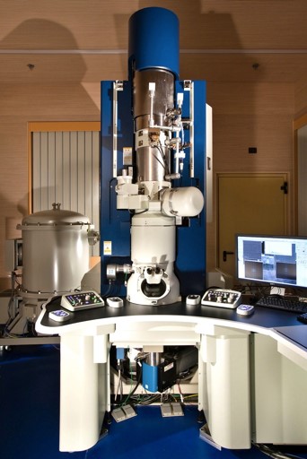
Transmission electron microscopy lab – Refs.: C. Bongiorno, S. Pannitteri, G. Nicotra (corrado.bongiorno@imm.cnr.it, salvatore.pannitteri@imm.cnr.it, giuseppe.nicotra@imm.cnr.it)
The electron microscopy center of Catania consists of a set of three laboratories, plus a specimens preparation lab, for the study of the structural and chemical-physical properties of materials with electron microscopy techniques at extremely high spatial resolution (0.65 Angstrom) based on unique instrumentation. In particular, the lab has three transmission electron microscopes equipped with Cold FEG (high brightness and highest monochromaticity, 0.26eV), FEG (high brightness and high monochromaticity, 0.7) and LaB6 (high brightness) electron probe, respectively.
The most performing microscope is the JEOL ARM200F and is equipped with a spherical aberration corrector on the electron probe so as to ensure a spatial resolution below the Angstrom in scanning transmission electron microscopy (S/TEM), even at very low energy, and in the energy range comprised between 200 KeV and 40KeV. This microscope is capable to analyse 2D materials, at atomic resolution, such as graphene, phosphorene, MoS2, etc. The instrument is equipped with three digital cameras, 2k x 2k, for wide angle diffraction, high resolution TEM and 5 STEM detectors for atomic resolution STEM analyses. It is also capable of performing tomographic analysis of nano-structured materials in both TEM that STEM mode. The instrument is also equipped with a last generation of monocromated electron energy loss spectrometer (EELS) and a large angle SDD-EDS x-ray detector (0.98 str), able to work simultaneously and acquire up to 1500spectra / sec in joint fast EELS / EDX mode.
The second microscope is a JEOL 2010F and equipped with a spectrometer GIF 2001 with advanced STEM-EELS spectrum imaging capabilities, two 2k x 2k digital cameras and BF / HAADF detectors for wide angle diffraction, high resolution TEM and STEM analyses respectively.
The third microscope is a JEOL 2010 and is equipped with a digital camera 1k x 1k, for high resolution TEM images and a EDS x-ray detector, Oxford x-sight 6498.
The center allows to perform accurate structural and chemical analysis at atomic resolution, making the achievement of significant advances at atomic-level possible, and in particular shed light on the properties of the materials of interest for photovoltaics, PCM and for new applications in microelectronics, nanoscience and nanotechnology.
The Lab is also equipped with facilities for mechanical and ion milling for the samples (disc grinder, dimple grinder, ultrasonic cutter, Gatan PIPS and PIPSII system, etc.), and several specimen holder for in-situ and temperature controlled TEM-S/TEM analyses area available.