

Dye (DSC) and Perovskite (PSC) solar cells are revolutionizing views and perspectives in the photovoltaics field so that their efficiency has been raised up to ~22% in only 8 years since the first intuition of prof Miyasaka that faced up to the limit of the absorption capability of the dyes with the high wide-ranging absorption coefficient of photoactive CH3NH3PbI3 perovskites. The two technologies bring us beyond silicon and are prospected to have a large dissemination in the society due to the low cost of materials and processes. Nevertheless, to match the ambitious requirements, a large effort is needed to optimize each component of the cell, especially at the photoanode side, starting from the transparent conductive oxide (TCO), going to the scaffold (TiO2) to end up with the light absorber.
In this framework, we deal with the growth and optimization of the photoanode in DSC and PSC, with approaches which are up-scalable and reliable to offer high throughput in view of the cost reduction.
ZnO:Al as TCO by sputtering methods
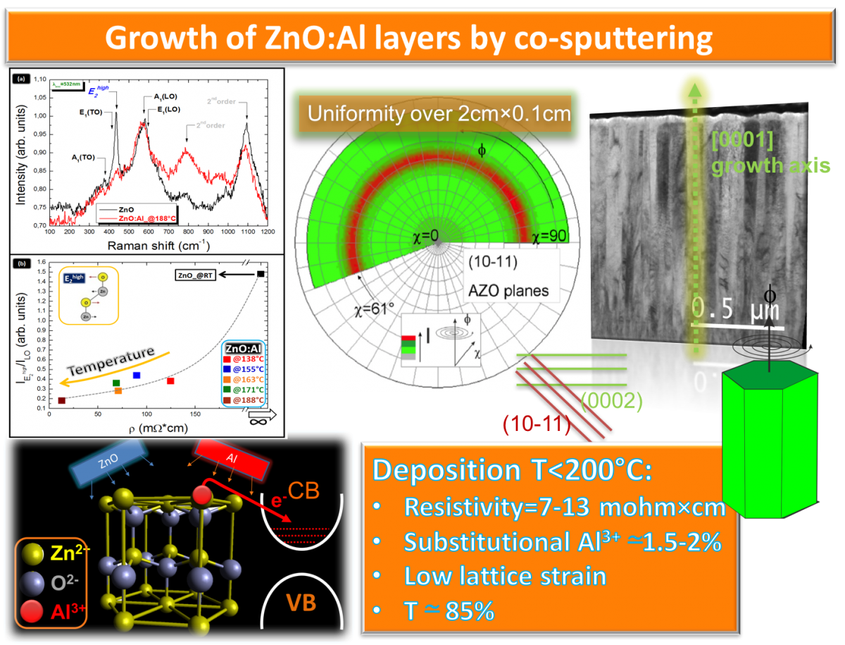
As the pervasive dissemination of the PV technology needs to firstly pass through a drastic cost reduction of the TCO, we focus our attention to implementable methods able to produce transparent conductive ZnO:Al layers at low temperature to replace FTO and ITO. To this intent, we apply an approach based on reactive magnetron co-sputtering deposition at effective deposition temperatures under 200°C. A full understanding of the role of all the involved deposition parameters allows a fine-tuning of the AZO lattice structure to incorporate an increasing amount of Al3+ species in the appropriate lattice position to be electrically active. Our AZO layers have transparency > 85% and resistivity under 10mohm×cm.
TiO2 compact and mesoporous layers by sputtering methods
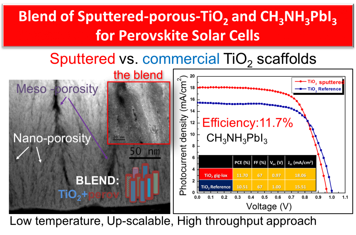
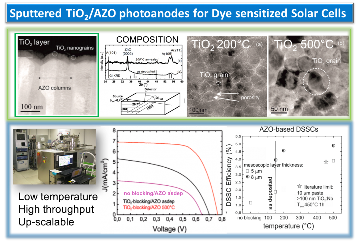
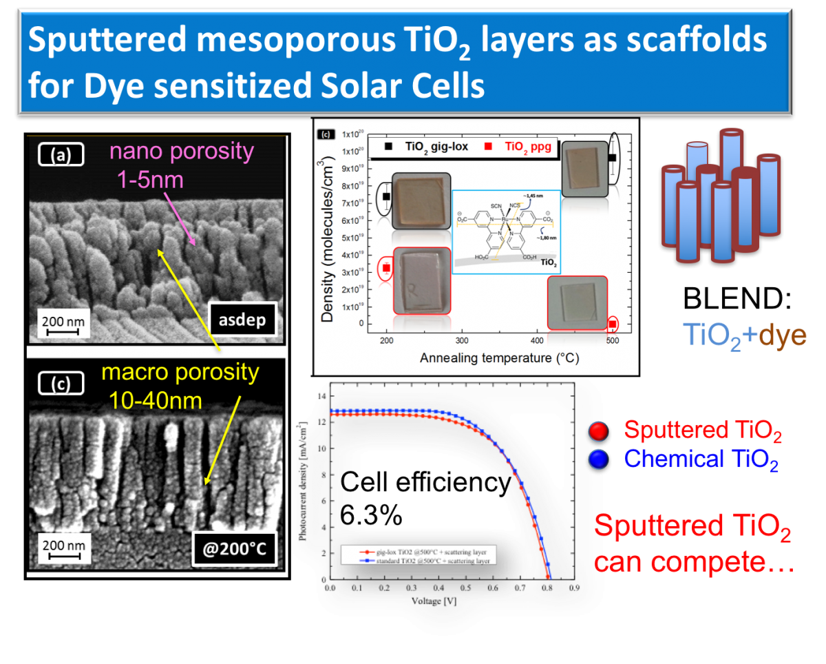
In DSC and PSC cell architecture, TiO2 represents a main actor since its role is twofold: as thin compact layer to block the recombination current; as mesoporous layer to act as scaffold for dye/perovskite loading and carrier extraction from the photoactive material. We deal with both components in the device by applying sputtering methods. Mesoporosity by conventional sputtering represents a challenge; thereby the need of innovative sputtering-based approaches, as those exploited in our laboratory in Catania Headquarters. which combines high deposition rates with the in-situ oxidation of the sputtered species. With this method, we grow, at RT, multi-porosity TiO2 layers with thickness from 150 to 1000 nm, transmittance >80%, porosity in the range of ~30-55% and high structural texturing
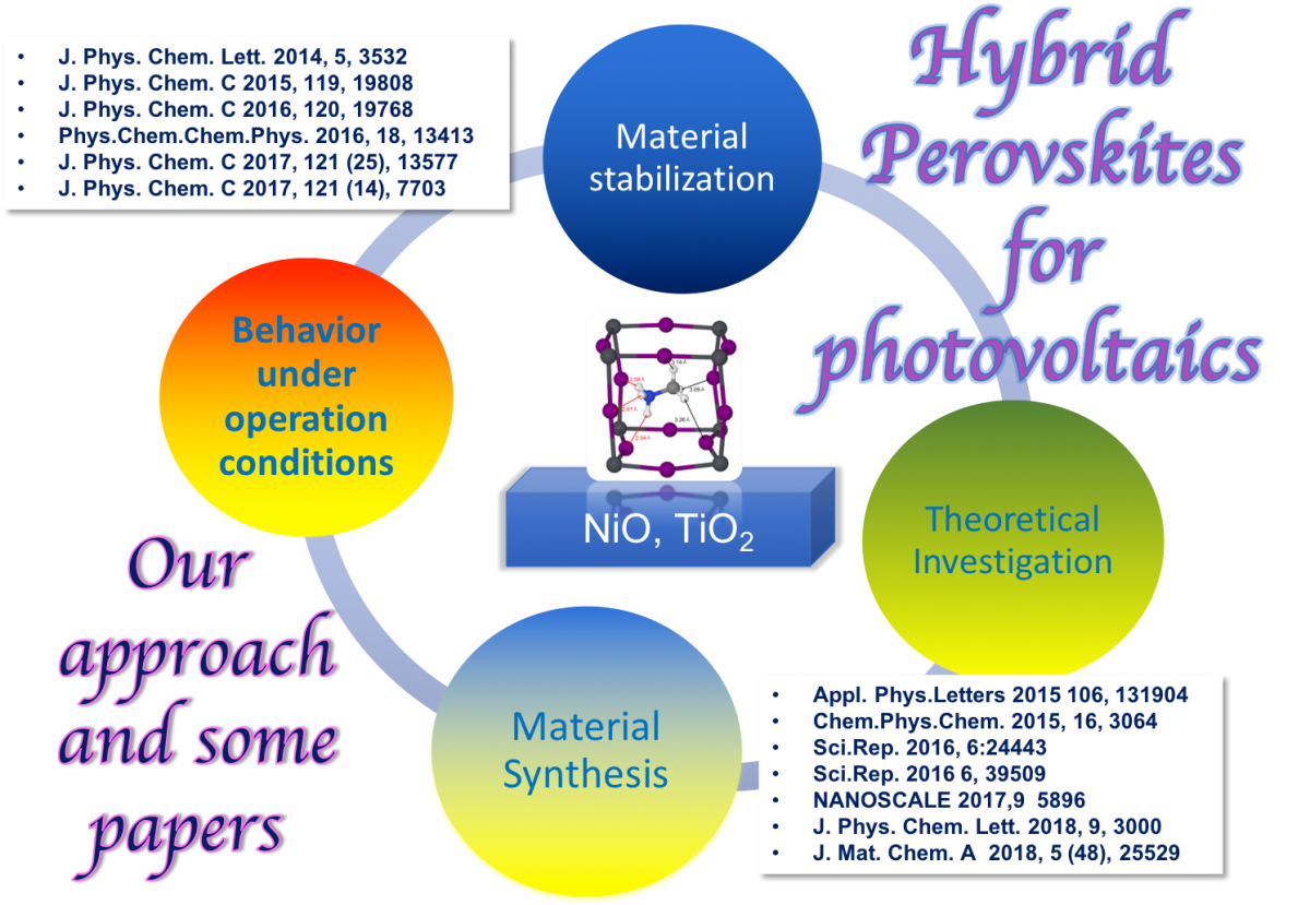
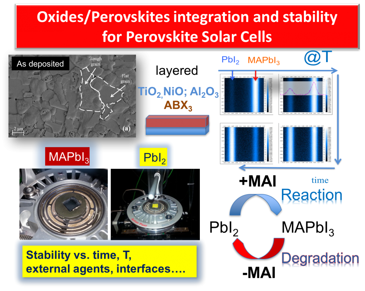
Hybrid perovksites
It is definitely clear that the advance of perovskite-based technologies is forced to pass through the rationalization of the assembling process as well as of the phenomena occurring into the lattice under conditions which mimic the material operation (illumination, temperature, interfaces, external species etc).
In this framework, we focus on the investigation of layered (p-i-n) and nanostructured blends of Hybrid Halides Perovskites with particular focus on: the early stage of the assembly; the stability of the atomic architecture; the changes at the operation conditions; strategies for stabilization and durability.
download the first Ph.D thesis on Hybrid Photovoltaics @IMM:
https://hq.imm.cnr.it/articles/first-phd-thesis-hybrid-photovoltaics-imm
contact person: Alessandra Alberti, alessandra.alberti@imm.cnr.it