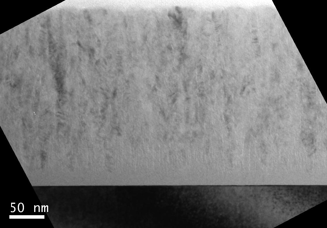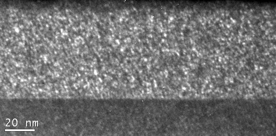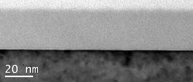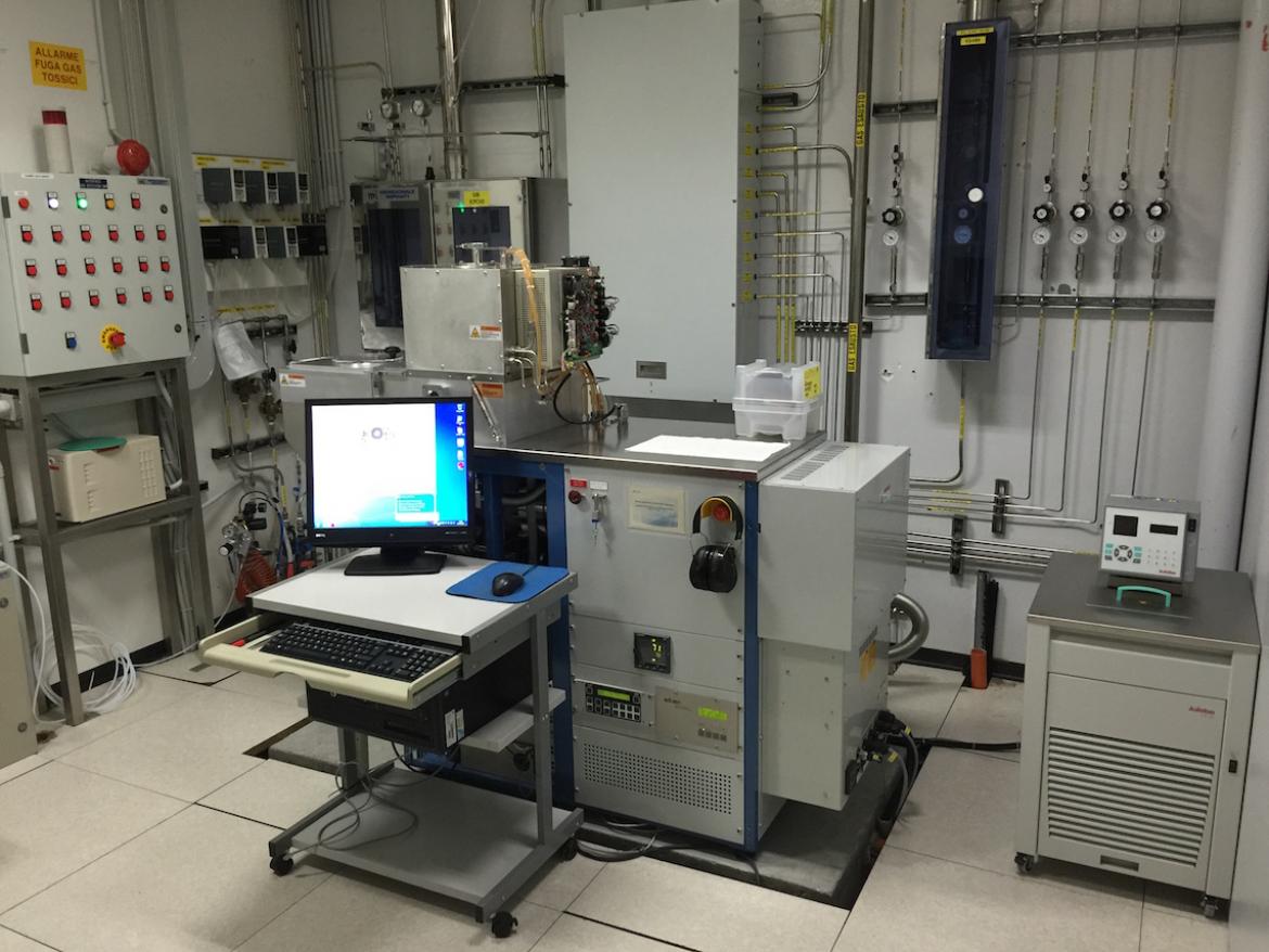
We exploit the capabilities of plasma to produce advanced materials for several applications ranging from amorphous solar cells, HIT solar cells, to advanced nanocsryalline materials to be integrated in state of the art devices. High density plasmas are particularly suitable for low temperature applications on flexible and low cost substrates being possible to deposit at temperature so low as 100°C layers with excellent electro-optical properties. The plasma technology is particularly appreciated for its compatibility with device production lines and its flexibility in terms of throughput. It is actually possible to prepare Si based and C based materials, eventually doped with P or B, like a-Si but also a-SiC and oxynitrides/oxycarbide SiOxNyCz. Most common applications of these materials are photovoltaic devices and thin film transistors.
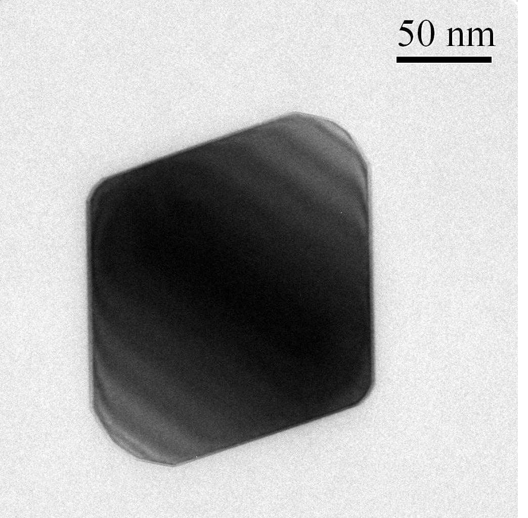
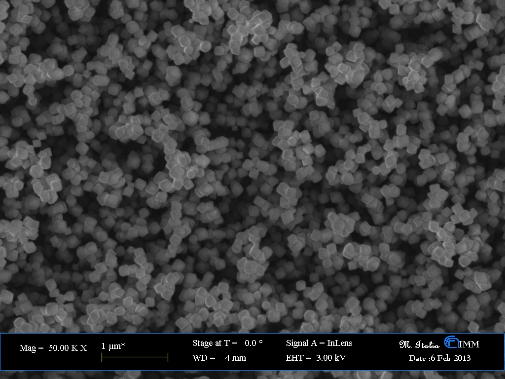
Depending on the pressure in the chamber, also large, octahedral Silicon nanocrystals are synthesized. These nanocsyrtals in the 100nm range and are excellent light traps and scattering centres. Thick layers of these nanoparticles show very intense photolumescence.
G.Faraci, A.R. Pennisi, A.Alberti, R.Ruggeri & G.Mannino* Giant photoluminescence emission in crystalline faceted Si grains SCIENTIFIC REPORTS | 3 : 2674 | DOI: 10.1038/srep02674
G.Mannino*, A.Alberti, R.Ruggeri, S.Libertino, A.R.Pennis & G.Faraci Octahedral faceted Si nanoparticles as optical traps with enormous yield amplification SCIENTIFIC REPORTS | 5 : 8354 | DOI: 10.1038/srep08354
E.M.L.D de Jong, G.Mannino*, A.Alberti, R.Ruggeri, M.Italia, F.Zontone, Y.Chushkin, A.R.Pennisi, T.Gregorkiewicz & G.Faraci Strong infrared photoluminescence in highly porous layers of large faceted Si crystalline nanoparticles SCIENTIFIC REPORTS | 6:25664 | DOI: 10.1038/srep25664
M.Mikolásek, M.Nemec, J.Kovác, M.Foti, C.Gerardi, G.Mannino, L.Valenti, S.Lombardo The influence of post-deposition annealing upon amorphous silicon/crystalline silicon heterojunction solar cells Materials Science and Engineering B 189 (2014) 1–6
Contact person: Giovanni Mannino (giovanni.mannino@imm.cnr.it)
