

One of the prime applications for novel two-dimensional (2D) materials is their use in flexible electronics. In fact, one of the main characteristics of this new class of materials (graphene, metal dichalcogenides etc.) is their ability to preserve most of their structural and electronic characteristics upon bending or stretching. The excellent electronic and mechanical properties of 2D materials make them ideal for deposition on flexible substrates and their use in novel flexible devices.
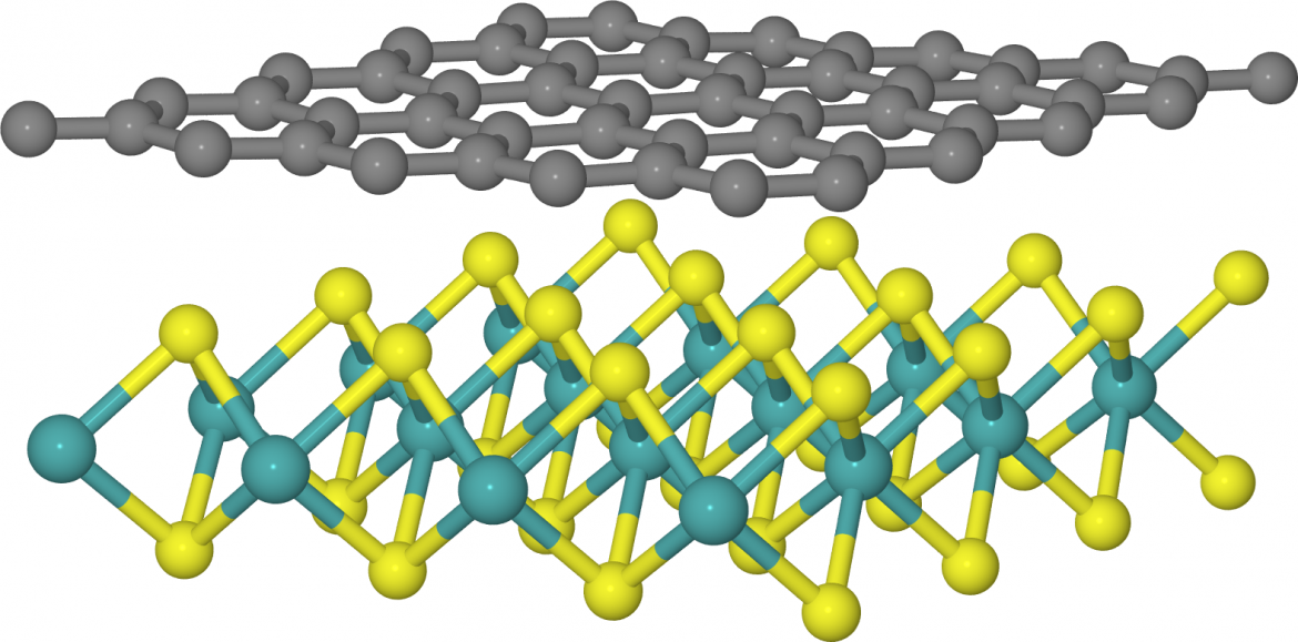
Semi-metallic graphene (Gr) and semiconducting transition metal dichalcogenides (MoS2, MoSe2, WS2, WSe2, …) are currently the object of interest for the fabrication of electronic/optoelectonic devices and sensors on flexible substrates. A research activity focused on the development of Gr-based field effect transistors on plastics (PEN, polymmide, …) is currently in progress at IMM HQ in Catania, in close collaboration with STMicroelectronics and in the framework of the Graphene Flagship. In this context, several critical scientific and technological steps for the fabrication of flexible Gr transistors on wafer scale have been addressed and/or are currently object of investigation, such as:
- optimized transfer methods of CVD grown Gr from metals to the target substrate;
- growth of high-k dielectrics (Al2O3) thin films at low temperatures (down to T=100°C) compatible with the plastic substrate by plasma-assisted atomic layer deposition.
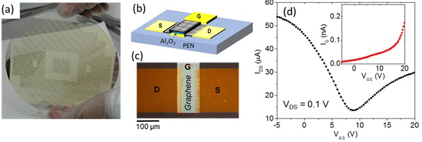
Fig.1 (a) Photograph of a 150 mm PEN substrate with Gr devices. (b) Schematic and (c) optical image of the channel region of a back-gated Gr transistor. (d) Measured transfer characteristic and leakage current (insert) on this device.
As a natural extension of this activity, a study of the main processing steps (contacts, dielectrics, doping, ...) for the fabrication of field effect devices based on MoS2 both on rigid and on flexible substrates has been also initiated.
In addition to the experimental research, a consolidated theoretical/computational activity takes place at the IMM HQ through state-of-the-art multiscale methodologies. We employ density functional theory calculations for the determination of the structural and electronic properties of two-dimensional materials. We use the non-equilibrium Green’s function formalism for the calculation of the quantum transport in devices based on 2D systems. Finally, we develop advanced kinetic Monte Carlo algorithms for the study of the evolution of growth processes regarding 2D materials. Our applicative focus is on the functionalization and the defects present in 2D materials, their interactions with various substrates, their electrical and device properties and finally, the simulation of their growth processes and atom/defect kinetics.
Reference persons: Antonino La Magna (theoretical), Filippo Giannazzo (experimental)