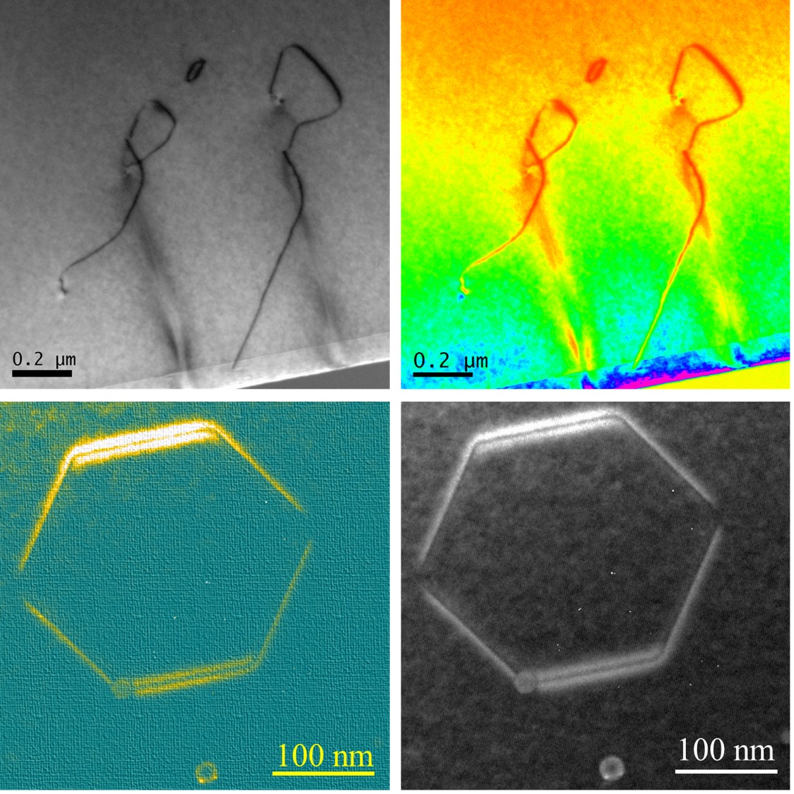
A defect is a fault or imperfection in a person or thing. This is the meaning given by the Collins vocabulary that associates a negative common sense to things which move away from perfection. This fits particularly well in material science, where we usually refer as lattice defects those atomic structures which perturb the long range crystallographic order. Since the structural, optical and electronic properties of materials and devices are detrimentally influenced by the presence of these defects, a deep knowledge of their formation and evolution is critical. However, by thinking with a different perspective, lattice defects can be considered as an amazing way in which matter reorganize itself after a perturbation. In this context, Transmission Electron Microscopy-related techniques have been recognised as the most performing tools to investigate matter below the nanoscale. In the talk, I will give an overview of my contribution by means of TEM, associated with complementary techniques, to a deep investigation of defects in nanostructures and thin films spanning from silicon, to germanium and silicon carbide.

