
Doping is the cornerstone of semiconductor technology with the possibility to finely tune the electrical response of these materials by changing the average concentration of dopants in the semiconductor matrix. Due to the aggressive scaling of microelectronic devices new opportunities opened up about the control of single charges and spins on individual dopants in silicon: silicon chips with ordered arrays of single dopant atoms could become the material of choice for quantum devices exploiting single donor spins as qubits. To achieve this goal, both deterministic incorporation of individual donors in silicon as well as localization of impurity dopants with high spatial accuracy is necessary. In this talk I will present an overview of our most recent results about the development of a deterministic doping technology based on the integration of different self-assembly materials.
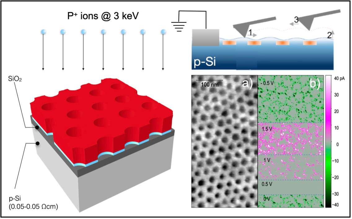
In particular, ultra-low energy ion implantation of P ions has been used to form a phosphorus d-layer in the sub-surface region of a highly resistive silicon substrate. Low temperature magnetoresistance measurements showed clear signature of weak antilocalization phenomena, that are undoubtedly connected to spin orbit interaction, suggesting important opportunities in quantum computation. Combining ultra-low energy ion implantation and mesoporous polymeric templates a periodic distribution of dopant impurities in the near-surface region of a Si wafer is obtained.1–3. In alternative, polymers terminated with a phosphorus containing moiety are used to create a d-layer source of dopants at the interface between a SiO2 capping layer and the underlying Si substrate.4 Subsequent driven-in of the phosphorus atoms into the silicon substrate is promoted by means of a high temperature annealing, achieving full activation of dopant impurities.5–7 This alternative approach for ex-situ doping of semiconductors guarantees an efficient and precise control of dopant concentration in the silicon substrate, offering the possibility to investigate dopant activation in ultrathin silicon on insulator substrates. The proposed technology is fully compatible with mass production of advanced microelectronic components, representing a simple and low-cost alternative to complex and expensive top-down doping approaches. The integration of this doping technology with advanced lithographic processes is proposed as a possible route to achieve the goal of deterministic doping.
In conclusion, in this talk different strategies to control the distribution of dopants at the nanoscale will be presented and critically evaluated. The presented experimental results indicate the possibility to modify the potential landscape and conductivity of a semiconductor substrate at the nanoscale by a periodic modulation of dopant impurities, envisioning the possibility to promote engineering of the semiconductor band structure, synthesis of artificial crystals, or formation of quantum dot arrays in a semiconductor host matrix.
References:
(1) Castro, C.; Schamm-Chardon, S.; Pecassou, B.; Andreozzi, A.; Seguini, G.; Perego, M.; Benassayag, G. In-Plane Organization of Silicon Nanocrystals Embedded in SiO2 Thin Films. Nanotechnology 2013, 24 (7). https://doi.org/10.1088/0957-4484/24/7/075302.
(2) Castro, C.; BenAssayag, G.; Pecassou, B.; Andreozzi, A.; Seguini, G.; Perego, M.; Schamm-Chardon, S. Nanoscale Control of Si Nanoparticles within a 2D Hexagonal Array Embedded in SiO2 Thin Films. Nanotechnology 2017, 28 (1). https://doi.org/10.1088/0957-4484/28/1/014001.
(3) Kuschlan, S.; Chiarcos, R.; Laus, M.; Pérez-Murano, F.; Llobet, J.; Fernandez-Regulez, M.; Bonafos, C.; Perego, M.; Seguini, G.; De Michielis, M.; Tallarida, G. Periodic Arrays of Dopants in Silicon by Ultralow Energy Implantation of Phosphorus Ions through a Block Copolymer Thin Film. ACS Appl. Mater. Interfaces 2023. https://doi.org/10.1021/acsami.3c03782.
(4) Perego, M.; Seguini, G.; Arduca, E.; Nomellini, A.; Sparnacci, K.; Antonioli, D.; Gianotti, V.; Laus, M. Control of Doping Level in Semiconductors via Self-Limited Grafting of Phosphorus End-Terminated Polymers. ACS Nano 2018, 12 (1), 178–186.
(5) Perego, M.; Caruso, F.; Seguini, G.; Arduca, E.; Mantovan, R.; Sparnacci, K.; Laus, M. Doping of Silicon by Phosphorus End-Terminated Polymers: Drive-in and Activation of Dopants. J. Mater. Chem. C 2020, 8, 10229–10237.
(6) Perego, M.; Seguini, G.; Mascheroni, E.; Arduca, E.; Gianotti, V.; Laus, M. Doping of Silicon with Phosphorus End-Terminated Polymers: Source Characterization and Dopant Diffusion in SiO2. J Mater Chem C 2021, 9 (11), 4020–4028. https://doi.org/10.1039/D0TC06015A.
(7) Pulici, A.; Kuschlan, S.; Seguini, G.; Taglietti, F.; Fanciulli, M.; Chiarcos, R.; Laus, M.; Perego, M. Electrical Characterization of Thin Silicon-on-Insulator Films Doped by Means of Phosphorus End-Terminated Polymers. Mater. Sci. Semicond. Process. 2023, 163, 107548. https://doi.org/10.1016/j.mssp.2023.107548.